
Homepage › Forums › Articles › Hardware › Processors › Introductory Microprocessor Concepts
Tagged: chip, cpu, electronics, integrated-circuit, introduction, microprocessor, newbies, processing, processor
This topic was published by DevynCJohnson and viewed 1657 times since "". The last page revision was "".
- AuthorPosts
A microprocessor is a single integrated circuit (IC) that possess the abilities of a Central Processing Unit (CPU). Microprocessors are programmable chips that use digital/binary data.
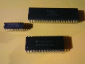

IC_Chips Microprocessors process data in binary form. Binary is a data representation in the form 0 and 1. These two digits are called binary bits. Each type of IC chip has a different way of representing 1 and 0 on a DC voltage. The binary bit 1 is represented by a logic high and 0 is a logic low.
Gate Type High Low TTL 0-0.5V 2.7-5V CMOS 0-1.5V 3.5-5V The clock rate is the frequency of the circuit's binary pulse. Since binary numbers are represented at the circuit level in the form of different voltages, the CPU must know the difference between a single 1 and two 1s next to each other. The clock rate indicates how quickly each bit is represented. A clock frequency of 1.2GHz (Gigahertz) or 1200MHz (Megahertz) means each binary bit is processed in 0.000000001 seconds. So, when the CPU reads a voltage, it knows that if it sees 5V in 0.000000001 seconds and then 5V in the following 0.000000001 seconds, the binary numbers read are "11".
NOTE: To convert frequency (in hertz) to time (in seconds), divide 1 by the clock speed. However, remember to first convert GHz to Hertz (GHz * 1000000000 = Hertz) and MHz to Hertz (MHz * 1000000 = Hertz). In summary, the equations are 1/Hertz or 1/(GHz * 1000000000).
Opcodes (operation code) are the set of codes/commands that make up the machine language. The Assembly programming language is the text-form of opcodes which is converted/compiled to the processor's opcode via an assembler. CPU chips read opcodes directly which are in binary.
A register is a small amount of data storage that resides on the chip. A collection of these registers forms a storage cache. The on-chip cache (such as the L2 cache) is significantly faster than the RAM. Many types of registers exist.
The term "Instruction Set Architecture" (ISA) or "Instruction Set" (IS) refers to the programming associated with a particular architecture. The programming includes address modes, data types, memory, interrupts, exceptions, opcodes, etc.
The term "microarchitecture" refers to the way the ISA is used on the particular CPU chip. The ISA (CPU programming) may be the same on various chips, but the data-flow may differ across the CPUs. The microarchitecture may differ to help save power, reduce heat, allow debugging, etc.
Operation
The CPU gets instructions from the main memory (RAM) and places it on the CPU cache (a collection of registers). The instructions are opcodes. The CPU decodes the opcodes and reads the instructions to see if any data must be retrieved. All needed data is retrieved. Next, the opcodes are executed. Lastly, the data is sent/written to the proper locations. The unneeded data on the cache is cleared. This cycle is repeated.
The repeated cycle discussed is known as the Instruction Cycle or the "fetch-and-execute cycle". This cycle is a little more complicated than what is mentioned above. However, those are the main events of the cycle.
Further Reading
- 8051 Microcontroller and Assembly - https://dcjtech.info/topic/8051-microcontroller-and-assembly/
- Quick x86 Assembly Info - https://dcjtech.info/topic/quick-x86-assembly-info/
- Hardware Registers - https://dcjtech.info/topic/hardware-registers/
- Microprocessor List (Wikipedia) - https://en.wikipedia.org/wiki/List_of_microprocessors
- List of Instruction Sets (Wikipedia) - https://en.wikipedia.org/wiki/List_of_instruction_sets
- Processors Reading Guide - https://dcjtech.info/topic/cpu-topics/
- Heptane CPU - https://dcjtech.info/topic/the-up-coming-heptane-cpu/
- AuthorPosts
